News Center
LATEST NEWS
- 016 DI-DO DC 24V IOS Android Smart Wifi Relay 2.4G RF Remote Control IOT Switch NPN IN Dry Contact Out Tuya Smart Life APP
- 024/8/16CH DI-DO CAN Relay Controller Module RS485 Digital NPN/PNP IO Expanding Board for CNC Car Automated Industry
- 03DC 12V 4CH MT8870 DTMF Tone Signal Decoder Phone Voice Remote Control Relay Switch Module For LED Motor Smart Home
- 04DC 12V 433M Wireless RS485 IO Point-to-Point Master-Slave RF Transceiver Relay Swicth Board for Water Pump LED PTZ PLC
- 05Serial Port Server Module RS485 to Ethernet Network TCP/IP Converter UDP TCP Client Server MQTT PLC
- 063.3V-24V 8A Isolation Flip-Flop Latch Switch Module Bistable Single Button LED Relay Solenoid Valve

Email: sales@hyzk-electronics.com
Phone: 0086 18682384515
Address: 3rd floor, Building 6, 30 Fortress Road, Gongming Street, Guangming District, Shenzhen 518106
Industry articles
HomeIndustry articlesDetails
PCB Prototying
Publish: 2023-11-17 21:10:07 Update: 2025-04-27 23:16:21 View: 2079
Concept and function of PCB processing
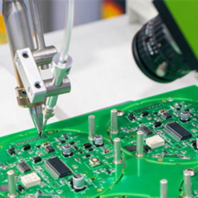
PCB processing and proofing refers to making a sample for customers and manufacturers to inspect, test and verify themselves before mass production of circuit boards.
This process usually includes designing schematic diagram, making PCB layout, printing circuit board, drilling and mounting components, and welding.
The purpose of PCB processing and proofing is to ensure that the circuit board functions normally, meets the customer's requirements, can be mass-produced,
and reduce the later production cost and time. Therefore, it plays a very important role in the development of electronic products.
1, the size and shape of the circuit board
Recommend